california nanosystems institute
Researchers Discover How to Make Ultra-Dense Nanowire Lattices
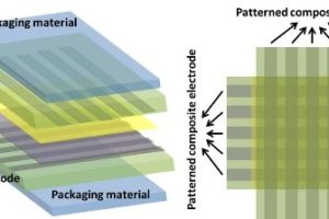
Researchers have invented a new technique for producing “Ultra High Density Nanowire Lattices and Circuits.” The method, for which a patent is pending, is akin to intaglio printmaking processes in which printing is done from ink below the surface of the plate. Intaglio processes emboss paper into the plate’s incised lines. The CNSI nanowires are like the embossed ink on a paper substrate, except that the nanowires are much, much smaller than ink lines. Take, for instance, a grid of crossed nanowires. Each cross represents the element of a simple circuit. The nanowire junction density reported in the “Science Express” article is in excess of 1011 per square centimeter.


