journal of applied physics


Making wafers faster by making features smaller
Washington, D.C. (December 14, 2010) — The manufacturing of semiconductor wafers used in all types of electronics involves etching small features onto a wafer with lasers, a process that is ultimately limited by the wavelength of the light itse…
Artificial black holes made with metamaterials
Washington, D.C. (November 16, 2010) — While our direct knowledge of black holes in the universe is limited to what we can observe from thousands or millions of light years away, a team of Chinese physicists has proposed a simple way to design an a…
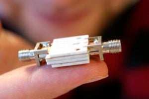
New way of detecting concealed radioactive material
Washington, D.C. (November 9, 2010) — Researchers at the University of Maryland have proposed a scheme for detecting a concealed source of radioactive material without searching containers one by one. Detection of radioactive material concealed in …