Humans have harnessed large portions of the electromagnetic spectrum for diverse technologies, from X-rays to radios, but a chunk of that spectrum has remained largely out of reach. This is known as the terahertz gap, located between radio waves and infrared radiation, two parts of the spectrum we use in everyday technologies including cell phones, TV remotes and toasters.
A theory developed by the late Stanford professor and Nobel laureate Felix Bloch suggested that a specially structured material that allowed electrons to oscillate in a particular way might be able to conduct these sought-after terahertz signals.
Now, decades after Bloch’s theory, Stanford physicists may have developed materials that enable these theorized oscillations, someday allowing for improvements in technologies from solar cells to airport scanners. The group published their findings in the Sept. 29 issue of Science.
Innovations in superlattice materials
Researchers have long thought that materials with repeating spatial patterns on the nanoscale might allow for Bloch’s oscillations, but technology is only just catching up to theory. Such a material requires that electrons travel long distances without deflection, where even the smallest imperfection in the medium through which the electrons flow can put them off their original path, like a stream trying to wind over and around rocks and fallen trees.
Burgeoning research in the field of two-dimensional materials and superlattices could make this type of material a reality. Superlattices are semiconductors made by layering ultra-thin materials whose atoms are arranged in a periodic lattice pattern.
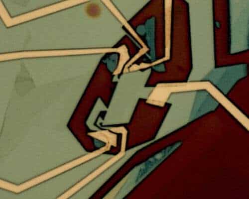
For this study, the researchers created a two-dimensional superlattice by sandwiching a sheet of atomically thin graphene in between two sheets of electrically insulating boron nitride. The atoms in the graphene and boron nitride have slightly different spacing, so when they are stacked on top of each other they create a special wave interference pattern called a moiré pattern.
New uses for electrons
Protected from air and contaminants by boron nitride above and below, electrons in the graphene flow along smooth paths without deflection, exactly as theory suggested would be needed to conduct terahertz signals. The researchers were able to send electrons through the graphene sheet, collect them on the other side and use them to thus infer the activity of the electrons along the way.
Usually, when a voltage is applied across a crystal, electrons are continuously accelerated in the direction of the electric field until they are deflected. In this moiré superlattice, researchers showed that the electrons can be confined to narrower bands of energy, said physics Professor David Goldhaber-Gordon, co-author of the study. Combined with very long times between deflections, this should lead the electrons to oscillate in place and emit radiation in the terahertz frequency range. This is a foundational success on the path toward creating controlled emission and sensing of terahertz frequencies.
In addition to bringing Bloch’s theory closer to reality, the researchers found a completely surprising change in the electronic structure of their superlattice material.
“In semiconductors, like silicon, we can tune how many electrons are packed into this material,” said Goldhaber-Gordon. “If we put in extra, they behave as though they are negatively charged. If we take some out, the current that moves through the system behaves as if it’s instead composed of positive charges, even though we know it’s all electrons.”
But this superlattice brings a new twist: Adding even more electrons produces particles of positive charge, and taking out even more returns to negative charge.
Future applications of this reversal in the character of the electrons could come in the form of more efficient p-n junctions, which are crucial building blocks to most semiconductor electronic devices such as solar cells, LEDs and transistors. Normally, if one shines light on a p-n junction, sending out one electron for every photon absorbed is considered excellent performance. But these new junctions could emit several electrons per photon, harvesting the energy of the light more effectively.
Terahertz and Stanford, past and future
While this new research hasn’t yet created a Bloch oscillator, the scientists have achieved the first step by showing that the momentum and velocity of an electron can be preserved over long times and distances within this superlattice, said Menyoung Lee, co-author of the study who conducted the research as a graduate student in the Goldhaber-Gordon Group.
“We apply the very first original lessons of solid-state physics that Felix Bloch figured out a long time ago, and it turns out we can use that to drive unique conduction phenomena in novel engineered materials,” Lee said.
Terahertz frequency technology could eventually be an improvement on today’s technologies. When U.S. airports scan passengers at security checkpoints today, they use microwaves, which penetrate nonmetal materials to reveal concealed metal objects. Goldhaber-Gordon explained that terahertz has similar transmission properties but shorter wavelength, potentially revealing even nonmetal concealed objects at high resolution. He added that terahertz scanners could also be used to detect defects such as hidden cavities in objects on a manufacturing assembly line.
The clean electronic conduction demonstrated in this work also furthered understanding of the ways in which electrons interact and flow, and Goldhaber-Gordon said his lab plans to use these insights to work on creating extremely narrow beams of electrons to send through superlattices. He called this new field “electron optics in 2-D materials” because these beams travel in straight lines and obey laws of refraction similarly to beams of light.
“This is going to be an area that opens up a lot of new possibilities,” said Goldhaber-Gordon, “and we’re just at the start of exploring what we can do.”
Additional authors of this paper, “Ballistic Miniband Conduction in a Graphene Superlattice,” are Patrick Gallagher of Stanford University, John R. Wallbank and Vladimir I. Fal’ko of University of Manchester, and Kenji Watanabe and Takashi Taniguchi of the National Institute for Materials Science in Tsukuba, Japan.
Funding came from the Air Force Office of Scientific Research and the Gordon and Betty Moore Foundation, and was performed in part in the Stanford Nano Shared Facilities.


