An international team led by the University of Chicago’s Institute for Molecular Engineering has discovered how to manipulate a weird quantum interface between light and matter in silicon carbide along wavelengths used in telecommunications.
The work advances the possibility of applying quantum mechanical principles to existing optical fiber networks for secure communications and geographically distributed quantum computation. Prof. David Awschalom and his 13 co-authors announced their discovery in the June 23 issue of Physical Review X.
“Silicon carbide is currently used to build a wide variety of classical electronic devices today,” said Awschalom, the Liew Family Professor in Molecular Engineering at UChicago and a senior scientist at Argonne National Laboratory. “All of the processing protocols are in place to fabricate small quantum devices out of this material. These results offer a pathway for bringing quantum physics into the technological world.”
The findings are partly based on theoretical models of the materials performed by Awschalom’s co-authors at the Hungarian Academy of Sciences in Budapest. Another research group in Sweden’s Linköping University grew much of the silicon carbide material that Awschalom’s team tested in experiments at UChicago. And another team at the National Institutes for Quantum and Radiological Science and Technology in Japan helped the UChicago researchers make quantum defects in the materials by irradiating them with electron beams.
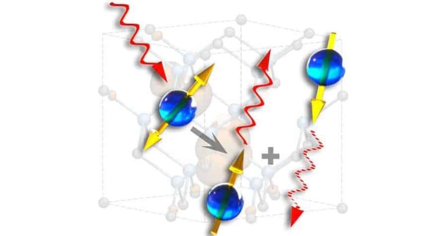
Quantum mechanics govern the behavior of matter at the atomic and subatomic levels in exotic and counterintuitive ways as compared to the everyday world of classical physics. The new discovery hinges on a quantum interface within atomic-scale defects in silicon carbide that generates the fragile property of entanglement, one of the strangest phenomena predicted by quantum mechanics.
Entanglement means that two particles can be so inextricably connected that the state of one particle can instantly influence the state of the other, no matter how far apart they are.
“This non-intuitive nature of quantum mechanics might be exploited to ensure that communications between two parties are not intercepted or altered,” Awschalom said.
Exploiting quantum mechanics
The findings enhance the once-unexpected opportunity to create and control quantum states in materials that already have technological applications, Awschalom noted. Pursuing the scientific and technological potential of such advances will become the focus of the newly announced Chicago Quantum Exchange, which Awschalom will direct.
An especially intriguing aspect of the new paper was that silicon carbide semiconductor defects have a natural affinity for moving information between light and spin (a magnetic property of electrons). “A key unknown has always been whether we could find a way to convert their quantum states to light,” said David Christle, a postdoctoral scholar at the University of Chicago and lead author of the work. “We knew a light-matter interface should exist, but we might have been unlucky and found it to be intrinsically unsuitable for generating entanglement. We were very fortuitous in that the optical transitions and the process that converts the spin to light is of very high quality.”
The defect is a missing atom that causes nearby atoms in the material to rearrange their electrons. The missing atom, or the defect itself, creates an electronic state that researchers control with a tunable infrared laser.
“What quality basically means is: How many photons can you get before you’ve destroyed the quantum state of the spin?” said Abram Falk, a researcher at the IBM Thomas J. Watson Resarch Center in Yorktown Heights, N.Y., who is familiar with the work but not a co-author on the paper.
The UChicago researchers found that they could potentially generate up to 10,000 photons, or packets of light, before they destroyed the spin state. “That would be a world record in terms of what you could do with one of these types of defect states,” Falk added.
Awschalom’s team was able to turn the quantum state of information from single electron spins in commercial wafers of silicon carbide into light and read it out with an efficiency of approximately 95 percent.
Millisecond coherence
The duration of the spin state—called coherence—that Awschalom’s team achieved was a millisecond. Not much by clock standards, but quite a lot in the realm of quantum states, in which multiple calculations can be carried out in a nanosecond, or a billionth of a second.
The feat opens up new possibilities in silicon carbide because its nanoscale defects are a leading platform for new technologies that seek to use quantum mechanical properties for quantum information processing, sensing magnetic and electric fields and temperature with nanoscale resolution, and secure communications using light.
“There’s about a billion-dollar industry of power electronics built on silicon carbide,” Falk said. “Following this work, there’s an opportunity to build a platform for quantum communication that leverages these very advanced classical devices in the semiconductor industry,” he said.
Most researchers studying defects for quantum applications have focused on an atomic defect in diamond, which has become a popular visible-light testbed for these technologies.
“Diamond has been this huge industry of quantum control work,” Falk noted. Dozens of research groups across the country have spent more than a decade perfecting the material to achieve standards that Awschalom’s group has mastered in silicon carbide after only a few years of investigation.
Silicon carbide versatility
“There are many different forms of silicon carbide, and some of them are commonly used today in electronics and optoelectronics,” Awschalom said. “Quantum states are present in all forms of silicon carbide that we’ve explored. This bodes well for introducing quantum mechanical effects into both electronic and optical technologies.”
Researchers now are beginning to wonder if this type of physics also may work in other materials, Falk noted.
“Moreover, can we rationally design a defect that has the properties we want, not just stumble into one?” he asked.
Defects are the key.
“For decades the electronics industry has come up with a myriad of tricks to remove all the defects from their devices because defects often cause problems in conventional electronics,” Awschalom explained. “Ironically, we’re putting the defects back in for quantum systems.”