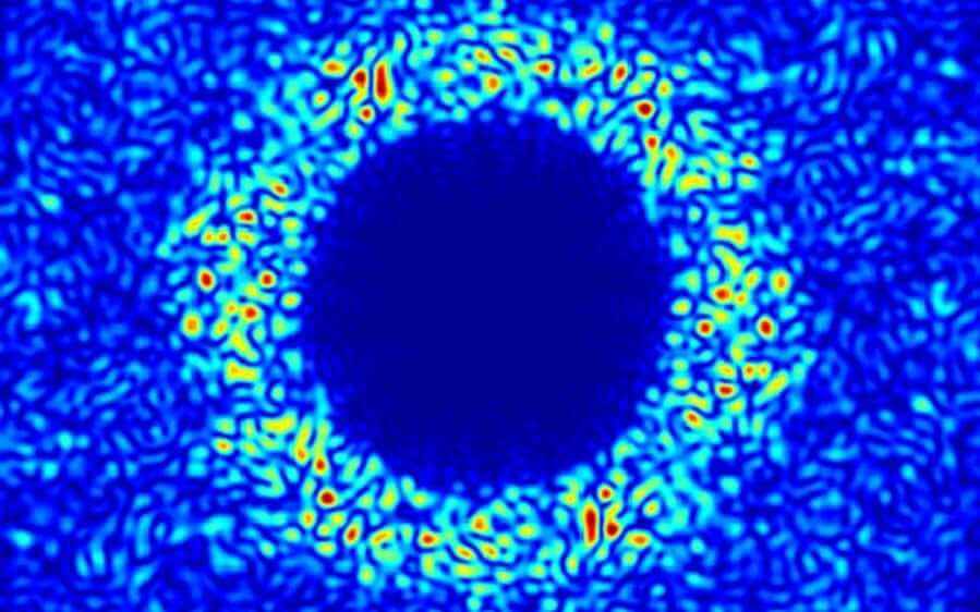
A team co-led team by the University of Surrey has successfully increased the levels of energy absorbed by wafer-thin photovoltaic panels by 25%.
Their solar panels, just one micrometre thick (1μm), convert light into electricity more efficiently than others as thin and pave the way to make it easier to general more clean, green energy.
In a paper published in the American Chemical Society’s Photonics journal, the team detail how they used characteristics of sunlight to design a disordered honeycomb layer which lies on top of a wafer of silicon. Their approach is echoed in nature in the design of butterfly wings and bird eyes. The innovative honeycomb design enables light absorption from any angle and traps light inside the solar cell, enabling more energy to be generated.
The team of researchers from the University of Surrey and Imperial College London worked with experimental collaborators at AMOLF in Amsterdam to design, model and create the new ultra-thin photovoltaic.
The team of researchers from the University of Surrey and Imperial College London worked with experimental collaborators at AMOLF in Amsterdam to design, model and create the new ultra-thin photovoltaic.
Dr Florescu continued, “There’s enormous potential for using ultra-thin photovoltaics. For example, given how light they are, they will be particularly useful in space and could make new extra-terrestrial projects viable. Since they use so much less silicon, we are hoping there will be cost savings here on Earth as well, plus there could be potential to bring more benefits from the Internet of Things and to create zero-energy buildings powered locally.”
As well as benefiting solar power generation, the findings could also benefit other industries where light management and surface engineering are crucial, for example, photo-electrochemistry, solid-state light emission and photodetectors.
Next steps for the team will include investigating commercial partners and developing manufacturing techniques.
Read the full paper here.


