In the ongoing quest to make electronic devices ever smaller and more energy efficient, researchers want to bring energy storage directly onto microchips, reducing the losses incurred when power is transported between various device components. To be effective, on-chip energy storage must be able to store a large amount of energy in a very small space and deliver it quickly when needed – requirements that can’t be met with existing technologies.
Addressing this challenge, scientists at Lawrence Berkeley National Laboratory (Berkeley Lab) and UC Berkeley have achieved record-high energy and power densities in microcapacitors made with engineered thin films of hafnium oxide and zirconium oxide, using materials and fabrication techniques already widespread in chip manufacturing. The findings, published in the journal Nature, pave the way for advanced on-chip energy storage and power delivery in next-generation electronics.
“We’ve shown that it’s possible to store a lot of energy in microcapacitors made from engineered thin films, much more than what is possible with ordinary dielectrics,” said Sayeef Salahuddin, the Berkeley Lab faculty senior scientist and UC Berkeley professor who led the project. “What’s more, we’re doing this with a material that can be processed directly on top of microprocessors.”
This research is part of broader efforts at Berkeley Lab to develop new materials and techniques for smaller, faster, and more energy-efficient microelectronics.
Capacitors are one of the basic components of electrical circuits but they can also be used to store energy. Unlike batteries, which store energy through electrochemical reactions, capacitors store energy in an electric field established between two metallic plates separated by a dielectric material. Capacitors can be discharged very rapidly when needed, allowing them to deliver power quickly, and they do not degrade with repeated charge-discharge cycles, giving them much longer lifespans than batteries. However, capacitors generally have much lower energy densities than batteries, meaning they can store less energy per unit volume or weight, and that problem only gets worse when you try to shrink them down to microcapacitor size for on-chip energy storage.
Here, the researchers achieved their record-breaking microcapacitors by carefully engineering thin films of HfO2-ZrO2 to achieve a negative capacitance effect. Normally, layering one dielectric material on top of another results in an overall lower capacitance. However, if one of those layers is a negative-capacitance material, then the overall capacitance actually increases. In earlier work, Salahuddin and colleagues demonstrated the use of negative capacitance materials to produce transistors that can be operated at substantially lower voltages than conventional MOSFET transistors. Here, they harnessed negative capacitance to produce capacitors capable of storing greater amounts of charge, and therefore energy.
The crystalline films are made from a mix of HfO2 and ZrO2 grown by atomic layer deposition, using standard materials and techniques from industrial chip fabrication. Depending on the ratio of the two components, the films can be ferroelectric, where the crystal structure has a built-in electric polarization, or antiferroelectric, where the structure can be nudged into a polar state by applying an electric field. When the composition is tuned just right, the electric field created by charging the capacitor balances the films at the tipping point between ferroelectric and antiferroelectric order, and this instability gives rise to the negative capacitance effect where the material can be very easily polarized by even a small electric field.
“That unit cell really wants to be polarized during the phase transition, which helps produce extra charge in response to an electric field,” said Suraj Cheema, a postdoc in Salahuddin’s group and one of the lead authors of the paper. “This phenomena is one example of a negative capacitance effect but you can think of it as a way of capturing way more charge than you normally would have.” Nirmaan Shanker, a graduate student in Salahuddin’s group, is co-lead author.
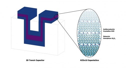
To scale up the energy storage capability of the films, the team needed to increase the film thickness without allowing it to relax out of the frustrated antiferroelectric-ferroelectric state. They found that by interspersing atomically thin layers of aluminum oxide after every few layers of HfO2-ZrO2, they could grow the films up to 100 nm thick while still retaining the desired properties.
Finally, working with collaborators at the MIT Lincoln Laboratory, the researchers integrated the films into three-dimensional microcapacitor structures, growing the precisely layered films in deep trenches cut into silicon with aspect ratios up to 100:1. These 3D trench capacitor structures are used in today’s DRAM capacitors and can achieve much higher capacitance per unit footprint compared to planar capacitors, allowing greater miniaturization and design flexibility. The properties of the resulting devices are record breaking: compared to the best electrostatic capacitors today, these microcapacitors have nine-times higher energy density and 170-times higher power density (80 mJ-cm-2 and 300 kW-cm-2, respectively).
“The energy and power density we got are much higher than we expected,” said Salahuddin. “We’ve been developing negative capacitance materials for many years, but these results were quite surprising.”
These high-performance microcapacitors could help meet the growing demand for efficient, miniaturized energy storage in microdevices such as Internet-of-Things sensors, edge computing systems, and artificial intelligence processors. The researchers are now working on scaling up the technology and integrating it into full-size microchips, as well as pushing the fundamental materials science forward to improve the negative capacitance of these films even more.
“With this technology, we can finally start to realize energy storage and power delivery seamlessly integrated on-chip in very small sizes,” said Cheema. “It can open up a new realm of energy technologies for microelectronics.”
Parts of this work were performed at the Molecular Foundry, a DOE Office of Science nanoscience user facility located at Berkeley Lab.
This research was supported by the Department of Energy’s Office of Science, Office of Basic Energy Sciences, the Defense Threat Reduction Agency (DTRA), and the Secretary of Defense for Research and Engineering.


