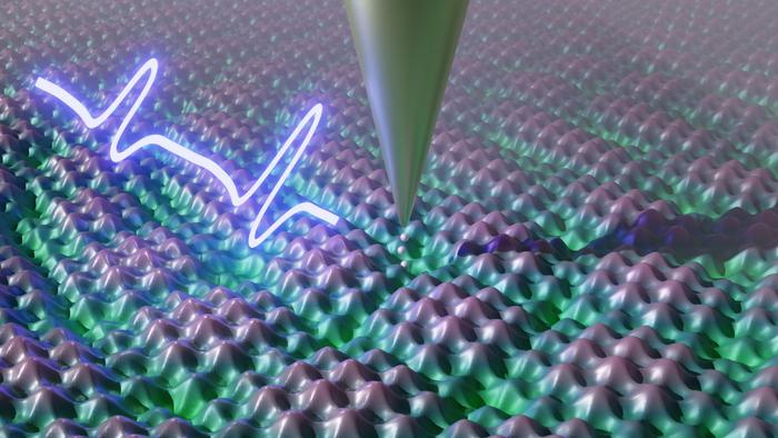
Scientists at the University of Stuttgart have developed a new microscopy technique that allows unprecedented visualization of electron movement in complex materials. The method could lead to breakthroughs in creating materials with customized properties for next-generation electronics and sensors.
The research team, led by Prof. Sebastian Loth at the Institute for Functional Matter and Quantum Technologies (FMQ), combined atomic-scale imaging with ultrafast spectroscopy to observe how impurities affect electron behavior at the nanoscale.
Picosecond Pulses Probe Atomic Interactions
The scientists studied a niobium-selenium compound exhibiting a phenomenon called a charge density wave – a collective oscillation of electrons. By applying extremely short electrical pulses lasting just one picosecond (a trillionth of a second), they were able to track how a single atomic impurity disrupts this wave.
“With the method we developed, we can make things visible that no one has seen before,” says Prof. Loth. “This makes it possible to settle questions about the movement of electrons in solids that have been unanswered since the 1980s.”
Atomic-Level Design for Macroscale Properties
The findings have significant implications for materials science and engineering. In advanced materials, tiny changes at the atomic scale can dramatically alter bulk properties – for instance, transforming insulators into superconductors.
“If we can understand how the movement of the electron collective is stopped, then we can also develop materials with desired properties in a more targeted manner,” Loth explains. “Design at the atomic level has a direct impact on the macroscopic properties of the material.”
The new technique achieves both high spatial and temporal resolution by combining a scanning tunneling microscope with pump-probe spectroscopy. To capture usable data, the experiment is repeated 41 million times per second.
“There are established methods for visualizing individual atoms or their movements,” explains Loth. “But with these methods, you can either achieve a high spatial resolution or a high temporal resolution.”
The research builds on work conducted at the Max Planck Institute for Solid State Research in Stuttgart and the Max Planck Institute for the Structure and Dynamics of Matter in Hamburg.
Prof. Loth, who has led the “Physics on the Atomic Scale” research group at FMQ since 2017, previously worked at IBM’s Almaden Research Center and received an ERC Starting Grant in 2015.
The new imaging capability could accelerate development of advanced materials for future sensors and electronic components requiring ultra-fast switching at the atomic scale.


