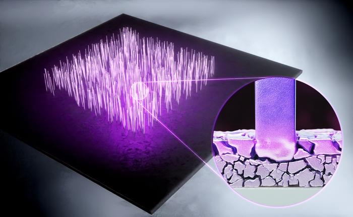
Summary: Researchers at Nagoya University have developed a new technique for mass-producing pure metal nanowires, potentially transforming the manufacturing of next-generation electronics.
Estimated reading time: 6 minutes
A team of scientists from Nagoya University in Japan has unveiled a novel method for growing metal nanowires (NWs) en masse, potentially solving a longstanding challenge in the field of nanotechnology. This breakthrough could pave the way for more efficient production of advanced electronics, including improved circuitry, LEDs, and solar cells.
Why it matters
Metal nanowires are crucial components in next-generation electronics due to their unique properties and minuscule size. However, their widespread adoption has been hindered by difficulties in mass production while maintaining quality and purity. This new technique could overcome these obstacles, potentially leading to more affordable and higher-performing electronic devices.
From Atoms to Forests: The Nanowire Growth Process
The research team, led by Yasuhiro Kimura at the Nagoya University Graduate School of Engineering, developed a method that uses atomic diffusion in a solid phase state, enhanced by ion beam irradiation, to create aluminum nanowires from single crystals.
“We realized mass growth of forest-like metallic NWs using only three key processes: thin film deposition on a substrate, ion beam irradiation, and heating,” Kimura explained. This approach differs significantly from traditional gas-phase methods, which have proven challenging for metal nanowire production.
Key steps in the process include:
- Thin film deposition: A layer of aluminum is deposited on a substrate.
- Ion beam irradiation: Crystal grains within the aluminum film are bombarded with ions, causing coarsening at the surface layer.
- Heating: The application of heat triggers an upward flow of atoms, resulting in nanowire growth.
The team’s innovative use of ion beam irradiation created localized regions of high stress within the aluminum film. These stressed areas served as pathways for atomic diffusion and provided nuclei and driving forces for vertical nanowire growth.
Impressive Results and Future Applications
The new technique yielded remarkable results, as Kimura noted: “We increased the density of aluminum NWs from 2×10⁵ NWs per square cm to 180×105 per square cm.” This nine-fold increase in density represents a significant step toward practical, large-scale production of metal nanowires.
The resulting aluminum nanowires possess several advantageous characteristics:
- Large surface area
- Good mechanical properties (due to their single-crystal structure)
- Resistance to natural oxidation
These properties make the nanowires particularly suitable for use in:
- Sensing devices
- Optoelectronics
- Gas sensors
- Biomarkers
Beyond Aluminum: Expanding the Technique
While the current study focused on aluminum, the researchers believe their method could be applied to other metals as well. “It can also be extended to other metals in principle,” Kimura stated. This versatility could significantly broaden the technique’s impact across various industries and applications.
Overcoming Previous Limitations
Prior attempts at mass-producing metal nanowires have faced several obstacles:
- Vapor pressure limitations
- Chemical reduction problems
- Difficulty in maintaining quality during scaling
The Nagoya University team’s approach addresses these issues by working with solid-state materials and controlling atomic diffusion within the film. This novel strategy circumvents many of the challenges associated with gas-phase production methods.
Looking Ahead: Implications for the Electronics Industry
The ability to mass-produce pure metal nanowires could have far-reaching effects on the electronics industry:
- More efficient manufacturing processes
- Potential cost reductions in advanced electronics
- Improved performance of nanodevices
- New possibilities for miniaturization and integration of components
As the demand for smaller, more powerful electronic devices continues to grow, this breakthrough in nanowire production could play a crucial role in meeting future technological needs.
While the research is still in its early stages, the potential applications are vast. From more sensitive environmental sensors to faster, more energy-efficient computer chips, the mass production of metal nanowires could be a key enabler for numerous technological advancements.
As with any new technology, further research will be needed to optimize the process for large-scale industrial applications and to explore its potential with a wider range of metals. However, this breakthrough represents a significant step forward in the field of nanotechnology and offers exciting possibilities for the future of electronics manufacturing.
Quiz: Test Your Understanding of Metal Nanowire Production
- What is the key innovation in the new nanowire production technique? a) Using gas-phase atomic transport b) Controlling atomic diffusion within a solid film c) Increasing the vapor pressure of metals d) Chemical reduction of metal compounds
- Which of the following is NOT mentioned as a potential application for the produced nanowires? a) Gas sensors b) Optoelectronics c) Biomarkers d) Quantum computers
- By how much did the researchers increase the density of aluminum nanowires? a) 2 times b) 5 times c) 9 times d) 18 times
Answer Key:
ScienceBlog.com has no paywalls, no sponsored content, and no agenda beyond getting the science right. Every story here is written to inform, not to impress an advertiser or push a point of view.
Good science journalism takes time — reading the papers, checking the claims, finding researchers who can put findings in context. We do that work because we think it matters.
If you find this site useful, consider supporting it with a donation. Even a few dollars a month helps keep the coverage independent and free for everyone.
- b) Controlling atomic diffusion within a solid film
- d) Quantum computers
- c) 9 times

