Take a sliver of molybdenum oxychloride, lay it on a chip of silicon, and turn it slowly under polarized light. At one angle it gleams back at you, bright and yellowish, every bit a metal. Rotate it ninety degrees and the shine drains away, replaced by the shifting colors of a transparent film. Same crystal, same light, utterly different behavior.
That trick has a name now, and numbers behind it. A team led by researchers at XPANCEO, working with colleagues at the National University of Singapore and the University of Chemistry and Technology in Prague, has measured exactly how this material, MoOCl2, splits and steers light. The verdict, published in Nano Letters, is that it bends light more sharply than any natural substance yet recorded across the visible and near-infrared range.
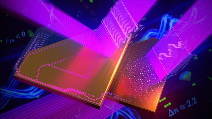
The reason lies deep in the crystal’s bones. MoOCl2 is what physicists rather grudgingly call a “bad metal,” shot through with one-dimensional chains of molybdenum atoms. Electrons race along those chains freely in one direction but get stuck going crosswise, which is why the material conducts roughly twelve times better along one axis than the other. That lopsidedness, baked into the atomic structure, is what gives the crystal its two faces: a metal one way, a dielectric (a transparent insulator, more or less) the other.
Physicists had clocked the strangeness of MoOCl2 before. Earlier studies, some in Science and Nature Communications, had actually watched tightly confined light waves snaking through it in highly directional ways.
But there was a gap, and an awkward one. Researchers could see what the material was doing, yet nobody had directly pinned down the underlying optical constants that govern it. Without those numbers, designing anything with confidence was a bit like trying to build a bridge while only guessing at the strength of your steel.
From watching to measuring
“Observing a phenomenon is the first step, but engineering requires precise numbers,” says Valentyn Volkov, founder and chief technology officer at XPANCEO and a corresponding author on the study. By measuring the complete dielectric tensor, his team says, they have handed the field the foundation it was missing.
So what did the numbers say? Using spectroscopic ellipsometry, a gold-standard technique, and backing it up with Mueller matrix and reflectance measurements, the team mapped the crystal’s response from the ultraviolet out to 1700 nanometres. They clocked an in-plane birefringence, the gap between how strongly the two axes bend light, of about 2.2. That is a record for a natural material, comfortably ahead of the usual suspects like calcite and rutile. And it means the kind of light manipulation that normally needs bulky optics could in principle be done with a flake thousands of times thinner than a human hair.
There was a second surprise tucked into the green part of the spectrum. At around 512 nanometres, one component of the crystal’s optical response very nearly drops to zero.
This is the so-called epsilon-near-zero, or ENZ, point, and it does something peculiar: light effectively slows down, while the electric field inside the material swells. Plenty of materials hit this condition, but usually in the deep ultraviolet or the mid-infrared, well away from where most lasers, cameras and sensors actually work. MoOCl2 does it slap in the middle of the visible.
That visible-range ENZ is the part that has photonics engineers paying attention, because it points toward chips where light is squeezed, routed and concentrated in tiny spaces and processed faster while burning less power. The material’s extreme anisotropy makes it a natural “hyperbolic” medium, which is jargon for a crystal that can funnel light into pencil-thin nanoscale rays without it scattering, a hard requirement if you want to shrink optical circuits. The researchers sketch out a wishlist of components: ultrathin broadband polarizers, waveguides that channel light through gaps smaller than conventional optics allow, and nonlinear devices that conjure up new colors of light. None of that is built yet. But the design rules now exist.
The lens that vanishes
And then there is the application that lends the whole thing a science-fiction shimmer. The same properties that make MoOCl2 attractive for photonic chips are precisely what you would want for the wafer-thin optics inside augmented-reality glasses, or, further out, a smart contact lens that overlays a display on the world without anyone noticing you are wearing it. The optics for that sort of device have to be reinvented at the atomic scale, because there is simply nowhere to hide a conventional lens. A crystal that can be a mirror or a window depending on which way you turn it, while being almost vanishingly thin, is a tantalizing place to start. Whether it survives the brutal journey from lab bench to mass production is, of course, another question entirely.
For now the achievement is quieter and more fundamental: a material whose two faces have finally been measured, not just glimpsed. The next move belongs to whoever decides to build something with it.
DOI / Source: 10.1021/acs.nanolett.5c06153
Frequently Asked Questions
Why does it matter that a crystal can be both a mirror and glass?
Because that extreme split is what lets the material bend and separate light far more sharply than ordinary optical materials, and in a layer thousands of times thinner than a hair. That opens a path to shrinking bulky optical components, like polarizers and waveguides, down to a scale that could fit on a chip or inside wearable displays.
Is it true this is the strongest light-bending effect in any natural material?
For the visible and near-infrared range, that is what the measurements show. The crystal’s in-plane birefringence of roughly 2.2 sits ahead of well-known anisotropic materials such as calcite and rutile, making MoOCl2 a new benchmark in this part of the spectrum.
What is an epsilon-near-zero point, and why is the green one a big deal?
It is a wavelength where the material’s optical response drops almost to zero, causing light to slow down and the electric field inside to intensify. Most materials reach this only in the ultraviolet or mid-infrared; MoOCl2 does it at around 512 nanometres, in visible green light, where lasers, microscopes and cameras already operate, which makes it far more useful for real devices.
Could this lead to smart contact lenses?
That is one of the long-term hopes, since wearable optics need light-steering parts at an almost invisible thickness. The study provides the design data rather than a finished device, so any contact lens or AR display is still some way off, pending the hard work of turning a lab material into manufacturable hardware.
ScienceBlog.com has no paywalls, no sponsored content, and no agenda beyond getting the science right. Every story here is written to inform, not to impress an advertiser or push a point of view.
Good science journalism takes time — reading the papers, checking the claims, finding researchers who can put findings in context. We do that work because we think it matters.
If you find this site useful, consider supporting it with a donation. Even a few dollars a month helps keep the coverage independent and free for everyone.