Skip to content
ScienceBlog.com
  • Featured Blogs
    • EU Horizon Blog
    • ESA Tracker
    • Experimental Frontiers
    • Josh Mitteldorf’s Aging Matters
    • Dr. Lu Zhang’s Gondwanaland
    • NeuroEdge
    • NIAAA
    • SciChi
    • The Poetry of Science
    • Wild Science
  • Topics
    • Brain & Behavior
    • Earth, Energy & Environment
    • Health
    • Life & Non-humans
    • Physics & Mathematics
    • Social Sciences
    • Space
    • Technology
  • Our Substack
  • Follow Us!
    • Bluesky
    • Threads
    • FaceBook
    • Google News
    • Twitter/X
  • Contribute/Contact

electronic devices

Professor Ly (back row, fourth from left) and her research team.

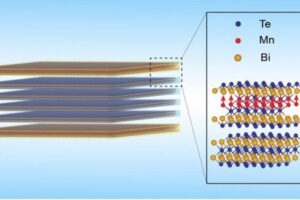
Novel Electric Field Discovery Points to Future of Quantum Computing, Nanotechnology

Four layers of a surface-conducting material (Bi2Te3) between two single layers of a magnetic insulator (MnBi2Te4). This structure creates the conditions to align the manganese spins (red arrows) and support a zero-resistance, spin-polarized current.

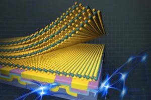
Could a Magnetic Sandwich Make Your Electronic Devices Work More Efficiently?

This artist’s rendition shows the newly developed integration platform. By engineering surface forces, researchers are able to directly integrate 2D materials into devices in a single contact-and-release step. Credits:Image: Courtesy of Sampson Wilcox/Research Laboratory of Electronics

Researchers safely integrate fragile 2D materials into devices

Substack subscription form sign up

Comments

  • Marco Messina on More Than a Third of Americans Have Lost Relationships Over Politics
  • Anon on Why Fructose Behaves Less Like a Calorie and More Like a Hormone
  • Mark Mellinger on Living Plastic Can Self-Destruct on Command
  • Marie Feret on The Silent Frequency That Makes Old Buildings Feel Haunted
  • Dax on The Silent Frequency That Makes Old Buildings Feel Haunted
© 2026 ScienceBlog.com | Follow our RSS / XML feed