Ask an AI assistant what a new beekeeper needs to know, and it will happily oblige. Handle the hive bodies, watch for swarming, learn the rhythms of the colony through the seasons. Plausible enough. The trouble starts when the question gets specific, when you want the answer pulled from a particular set of documents, filtered to a particular year, traced through the particular web of who-relates-to-what inside a company’s records. That is where today’s systems tend to wobble, and sometimes to invent.
That wobble has a name in the trade: hallucination. It is the polished, confident, entirely wrong answer, and it is the single biggest reason enterprises remain nervous about turning AI agents loose on their data.
A team at the Korea Advanced Institute of Science and Technology, KAIST, reckons the fix lies not in the language model at all but one layer down, in the database the model reaches into for facts. Most AI agents today run on a technique called retrieval-augmented generation, or RAG, which works by converting a question into numbers, finding documents that sit nearby in mathematical space, and handing those to the model as context. It is good at trawling unstructured text. It is rather worse at anything that also depends on relationships between entities, or on hard structured conditions like dates and categories. And real company data, of course, is all three of those things tangled together.
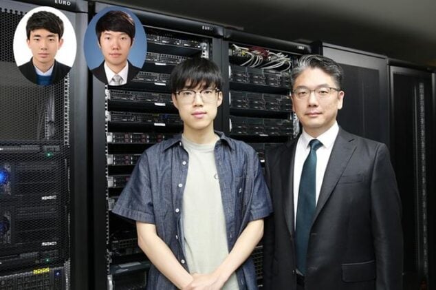
So the KAIST group, led by Min-Soo Kim of the School of Computing, built something that stops treating those three as separate problems. Their system, called AkasicDB, folds three kinds of database into one.
Three Stores, One Brain
Traditionally you would keep three specialists on the payroll. A vector database to judge what a document means; a graph database to map how people, companies and products connect; a relational database, the familiar tables-and-rows sort, to handle the structured stuff. Conventional setups either run all three as separate systems and stitch the answers together afterwards, or bolt graph and vector tricks onto an ordinary relational engine as add-ons that never quite belong. Both routes leak time and accuracy.
AkasicDB instead carries a vector store, a graph store and a relational store inside a single engine, sharing one query planner, so a question that needs all three can be answered in a single pass rather than three separate trips with the results bolted together at the end.
The retrieval method built on top of it, which the team calls Omni RAG, is the part that does the reasoning. Picture the kind of query a contracts lawyer actually asks: find the clauses involving a particular company among last year’s agreements, then explain how those clauses tie into a supply problem. To answer it properly you need vector search to grasp what the clauses mean, graph traversal to follow the connection to the supply issue, and relational filtering to throw out everything not signed last year. Pull only on the text, as a standard system does, and you get a fluent answer with the dates and the relationships quietly guessed. Which is precisely how a hallucination is born.
The system grew out of the group’s earlier work, a dual-store design named Chimera; AkasicDB is essentially Chimera with a native vector store grafted on, turning a two-part system into a three-part one and letting traversal, join and similarity search all run inside the same execution plan instead of being shuttled between separate programs.
Twenty Times Faster, and More Often Right
The numbers the team reported are not shy. In their experiments, complex searches that dragged on for as long as 21.3 seconds in existing systems came back in under a second, a speed-up of more than twentyfold. Accuracy of the AI’s responses improved by up to 78 per cent against conventional RAG. Tested across four bodies of knowledge, agriculture, computer science, law and a mixed bag, Omni RAG beat the vector-only approach every time, by margins running from a slim four points to a hefty twenty-eight, with the widest gap on the messiest, most cross-domain data. The pattern is telling: the more tangled the question, the more the integrated approach pulls ahead.
There are caveats worth keeping in view. This was a demonstration paper, presented on 2 June at SIGMOD, one of the database field’s marquee conferences, rather than a years-long deployment inside a working bank or factory. The accuracy was judged in part by another AI acting as referee, a method that tracks human opinion reasonably well but is not the same as it. And the speed figures were measured on a hefty server with a terabyte of memory, not the sort of kit most firms keep lying about.
Still, the bottleneck it targets is real. Once retrieval gets complicated, fetching the right facts can eat more time than the language model spends writing the answer, which rather upends the usual assumption that the model is the slow bit.
What KAIST is really proposing is a shift in where the intelligence of an AI agent lives. For years the race has been about bigger, cleverer models. Kim’s argument points the other way, towards the plumbing. “For AI agents to accurately understand and utilize the vast amounts of data held by enterprises, data infrastructure capable of processing vector, graph, and relational data in an integrated manner within a single system is essential,” he said. He frames AkasicDB as core infrastructure for the age of AI agents, with defence, manufacturing, finance, law and the sciences among the fields he expects to lean on it, exactly the high-stakes places where a confident fabrication does the most damage.
Whether the wider industry rebuilds its foundations to match is another matter, and a costly one; databases are not swapped out on a whim. But if the way to stop an AI making things up turns out to be a better-organised memory rather than a bigger brain, the beekeeper’s question may have been the easy part all along.
DOI / Source: https://doi.org/10.1145/3788853.3801609
Frequently Asked Questions
Why do AI assistants hallucinate in the first place?
Most AI agents answer by retrieving documents that look mathematically similar to your question and feeding them to a language model. That works for plain text, but when an answer also depends on relationships between entities or on structured conditions like dates and categories, the system often has nothing solid to ground those parts on, so it fills the gaps with plausible guesses. Those confident-sounding gaps are hallucinations.
How does combining three databases actually reduce errors?
AkasicDB keeps a vector store, a graph store and a relational store inside one engine, so a single query can search by meaning, follow connections between entities, and filter by hard facts such as dates all at once. Because the system retrieves grounded evidence from all three at the same time rather than guessing the structured parts, there is less room for the model to invent. KAIST reported accuracy gains of up to 78 per cent over conventional retrieval.
Is the twenty-times speed-up something ordinary companies would see?
The figures come from a controlled experiment on a powerful server with a terabyte of memory, comparing complex queries that took up to 21.3 seconds elsewhere against under a second on AkasicDB. Real-world results would depend heavily on the hardware, the data and the queries involved, so the headline numbers are best read as a demonstration of the approach rather than a guarantee.
Could this be used in fields like finance or law?
Those are exactly the areas the researchers have in mind, alongside defence, manufacturing and the sciences, because they combine large document archives with strict requirements for accuracy. In settings where a confidently wrong answer carries real consequences, grounding responses in relationships and structured data rather than text alone is the whole point.
What’s stopping every company from adopting this tomorrow?
For now AkasicDB has been shown off as a demonstration at an academic conference, not battle-tested inside a working enterprise over months or years. Swapping out a database is also a heavy, expensive undertaking, so even a promising design has to clear a high bar before businesses rebuild their data foundations around it.
ScienceBlog.com has no paywalls, no sponsored content, and no agenda beyond getting the science right. Every story here is written to inform, not to impress an advertiser or push a point of view.
Good science journalism takes time — reading the papers, checking the claims, finding researchers who can put findings in context. We do that work because we think it matters.
If you find this site useful, consider supporting it with a donation. Even a few dollars a month helps keep the coverage independent and free for everyone.