

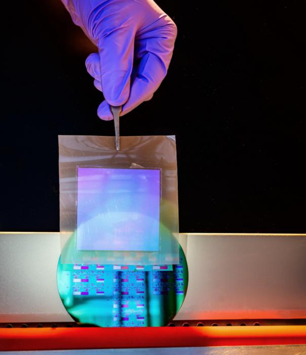
The transistor has stopped shrinking. Not slowing down, not easing off, but actually hitting a wall set by the size of atoms and the rules of quantum mechanics. For roughly sixty years the whole logic of computing rested on making these tiny switches smaller and cramming more of them onto a flat sheet of silicon. It worked spectacularly well. It worked so well that the industry painted itself into a corner.
So a team at the University of Illinois Urbana-Champaign has done the obvious thing, which also happens to be the very hard thing. Instead of going smaller, they went up.
Their idea, reported in Nature, is to stack working layers of silicon circuitry directly on top of one another, like floors in a building, with each tier holding its own transistors and wiring threading vertically between them. Qing Cao, the materials scientist who led the work, reaches for an architectural image to explain why this helps. “It’s like replacing a sprawling suburb with high-rises,” he says. You get the same functionality in a much smaller footprint, and the signals between floors travel shorter distances, which means faster and more efficient communication.
This matters because the old plan is running out of room. “In a sense, we’re hitting a limit imposed by physics,” Cao says.
The trouble is heat. Making good crystalline silicon and then carving high-performance transistors out of it normally demands temperatures close to 1,000 degrees Celsius. That’s fine for the first, bottom layer, when there’s nothing above it to ruin. But once you’ve laid down a floor of circuits with delicate metal wiring running through it, you cannot blast the next floor with that kind of heat without melting everything underneath. The industry’s accepted ceiling for any layer beyond the first is 400 degrees. A strict budget, and silicon has never much liked staying under it.
Why the upper floors kept disappointing
People have tried to dodge the problem for years by building those upper layers out of something other than proper single-crystal silicon: polycrystalline silicon, various metal oxides, carbon nanotubes, the fashionable two-dimensional semiconductors. All of them can be made at lower temperatures. And all of them, so far, have turned out worse than the silicon transistors sitting on the ground floor, hobbled by defects or by the limits of the materials themselves. That mismatch quietly cancels out most of the benefit you were hoping to get from stacking in the first place.
The Illinois approach sidesteps the whole dilemma with a bit of sleight of hand. Rather than grow the hot silicon in place, the team grows it somewhere else, peels it off as an extraordinarily thin sheet, and lays it down cold.
The sheets are nanomembranes of single-crystalline silicon, 10 nanometres thick or less. (For comparison, a normal silicon wafer runs 500 to 700 micrometres, tens of thousands of times thicker.) These films are released from a donor wafer, picked up, and transfer-printed onto the receiving chip using a roll laminator, the bonding step needing no more than about 200 degrees. Because the membranes are so thin they’re floppy, mechanically flexible, able to drape over whatever’s beneath them. “This conformality helps avoid interfacial defects like voids,” Cao notes, the kind of flaws that plague attempts to clamp two rigid wafers together.
Then there was the matter of the transistors themselves. Building a conventional transistor means “doping” silicon, introducing impurities to tune its electrical behaviour, and doping is yet another high-temperature step, often above 600 degrees. So the team used a design called a junctionless transistor, in which the silicon is doped uniformly and heavily before it’s ever stacked. No hot processing afterwards, no abrupt junctions to form. Because the film is so thin, the gate can still switch the channel on and off cleanly. Using all this, they built three stacked layers, each carrying 625 transistors, and wired them together into working logic gates and memory cells. Yields ran from 96 to 100 per cent across some 3,750 devices, and the transistors pushed currents above 650 microamps per micrometre, comfortably in the range of ordinary silicon made the hot way, and several times better than the alternative-material rivals.
Numbers like that, from an academic cleanroom rather than a billion-dollar fab, are what tend to make the chip industry sit up.
There are caveats, naturally. The device-to-device variability is still higher than a commercial foundry would tolerate, something the team attributes to the limits of their university facilities rather than the method itself. And the gate insulation is thicker than in the most advanced production chips, so the transistors need a touch more voltage to drive. Fixable problems, probably, but problems all the same.
What a chip foundry would want to know
What makes the result interesting beyond the lab is the timing. Vertical stacking is already creeping into commercial hardware, especially the specialised chips built for artificial intelligence, where shuttling data between memory and logic has become the real bottleneck. Shortening those journeys to a few hundred nanometres straight up, rather than millimetres across, is exactly the sort of thing that data-hungry AI workloads are starving for. The work was done inside a center whose industry partners include IBM, Intel and TSMC, and the team is now preparing to hand the process over to an actual foundry.
“But most importantly, we’ve shown that this process is scalable,” Cao says. Three tiers were a demonstration, not a ceiling. Whether the high-rise approach can climb to ten floors, or fifty, without the yields crumbling is the question that will decide if Moore’s law gets to keep going up after it ran out of room to go down.
DOI: 10.1038/s41586-026-10496-6
Frequently Asked Questions
Why can’t chipmakers just keep shrinking transistors like they used to?
Transistors have reached dimensions where the size of individual atoms and quantum-mechanical effects start to interfere with how they work, so shrinking them further stops delivering the old gains. That’s why engineers are now looking to build circuits upward in stacked layers instead of only outward across a flat surface. The shift could keep computing power growing even though the underlying switches aren’t getting any smaller.
Why is heat such a big obstacle to stacking chips?
Making high-quality silicon transistors normally requires temperatures near 1,000 degrees Celsius, but once a layer of circuits with metal wiring exists, anything above roughly 400 degrees would damage it. That tight thermal budget is what forced earlier attempts to use lower-quality materials for the upper layers. The Illinois method gets around it by growing the silicon elsewhere and bonding ultrathin sheets of it on at around 200 degrees.
How is this different from the 3D chips already on the market?
Current 3D chips are usually made by fabricating separate wafers and bonding them together, which leaves the connections between layers relatively coarse and sparse. The monolithic approach builds each layer directly on the one below, allowing far denser vertical connections aligned to within a few nanometres. That tighter integration is what unlocks much of the speed and efficiency advantage that stacking promises.
Could this actually end up in the computers and phones we buy?
It’s a strong possibility, though not imminent. The research was done with industry partners including IBM, Intel and TSMC, and the team is preparing to move the process into a commercial foundry. Real adoption will depend on whether the high yields hold up at industrial scale and across many more stacked layers than the three demonstrated so far.