Scientists have achieved one-nanometer optical resolution in a microscope that can visualize how light interacts with individual atoms and molecules.
The technique, called ultralow tip oscillation amplitude scattering near-field optical microscopy (ULA-SNOM), represents a dramatic leap forward in our ability to study materials at the smallest possible scales.
The international team combined atomic force microscopy with visible laser illumination and a specially prepared silver tip to create a confined light field just one cubic nanometer in volume. This breakthrough enables optical imaging of atomic-scale structures including single defects and molecules—something previously impossible with conventional optical methods.
Breaking the Diffraction Barrier
Traditional optical microscopy hits a fundamental limit called the diffraction barrier, restricting resolution to about 200 nanometers—roughly half the wavelength of visible light. The new technique shatters this limitation by confining light to spaces smaller than atoms themselves.
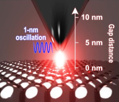
The key innovation involves oscillating a precisely fabricated silver tip with an amplitude of just one nanometer—about three atoms wide—over a sample surface. This creates what researchers call a “plasmonic cavity” where light becomes trapped and intensified in the tiny gap between tip and sample.
Working at ultrahigh vacuum and cryogenic temperatures of 8 Kelvin (-265°C), the team achieved unprecedented stability in maintaining the nanometer-scale gap necessary for atomic-resolution imaging. The extreme conditions prevent vibrations and contamination that would otherwise destroy the delicate light confinement.
Seeing Silicon Islands One Atom Thick
To demonstrate their technique, researchers imaged silicon islands just one atom thick on a silver surface. The material contrast was clearly visible despite the minuscule thickness, with the optical signal showing distinct differences between silicon and silver regions.
Key technical achievements include:
- Spatial resolution of 1 nanometer in optical imaging
- Detection of single atomic layer material differences
- Simultaneous electrical, mechanical, and optical measurements
- Stable operation in extreme cryogenic vacuum conditions
The team used focused ion beam polishing to shape their silver tip to nanometer precision, ensuring reproducible optical properties. This careful tip preparation proved crucial for achieving the extreme light confinement needed for atomic-scale resolution.
Three Views of the Same Atom
What makes ULA-SNOM particularly powerful is its ability to simultaneously measure electrical conductivity through scanning tunneling microscopy, mechanical forces via atomic force microscopy, and optical properties through light scattering. This triple perspective provides unprecedented insight into how atoms and molecules behave.
The researchers found that different harmonic frequencies of their oscillating tip revealed different aspects of the sample. Lower harmonics showed mainly topographic features, while higher harmonics—particularly the fourth harmonic—revealed true optical contrast between different materials.
By analyzing approach curves as the tip moved closer to the surface, the team could distinguish between electrical, mechanical, and optical signals, confirming that each measurement technique provided independent information about the sample’s properties.
Opening New Frontiers
The technique promises to transform our understanding of how light behaves at the atomic scale. Potential applications include studying photovoltaic materials, investigating quantum dots, and examining biological molecules at unprecedented resolution.
For materials science, ULA-SNOM offers the possibility of engineering optical properties at the atomic level by precisely controlling defects and interfaces. This could lead to new types of optical devices and more efficient solar cells.
The research demonstrates that by combining multiple advanced techniques—plasmonic enhancement, atomic force microscopy, and cryogenic conditions—scientists can push the boundaries of what’s possible in microscopy. The ability to see how individual atoms interact with light opens entirely new research directions in physics, chemistry, and materials science.
While the current setup requires specialized equipment and extreme conditions, the fundamental principles could eventually be adapted for broader scientific and industrial applications, bringing atomic-scale optical analysis closer to routine laboratory use.
ScienceBlog.com has no paywalls, no sponsored content, and no agenda beyond getting the science right. Every story here is written to inform, not to impress an advertiser or push a point of view.
Good science journalism takes time — reading the papers, checking the claims, finding researchers who can put findings in context. We do that work because we think it matters.
If you find this site useful, consider supporting it with a donation. Even a few dollars a month helps keep the coverage independent and free for everyone.