The circuits are so small they vanish from human sight, yet they could power the smartphones, cars, and aircraft of tomorrow. Johns Hopkins researchers have developed a new manufacturing process that creates microchip features smaller than 10 nanometers using materials that were previously incompatible with advanced production lines.
The breakthrough addresses a critical bottleneck in semiconductor manufacturing: traditional materials cannot withstand the high-powered radiation beams needed to etch ever-smaller details onto silicon wafers. The solution involves metal-organic compounds that absorb radiation more effectively than conventional resists.
“Companies have their roadmaps of where they want to be in 10 to 20 years and beyond. One hurdle has been finding a process for making smaller features in a production line where you irradiate materials quickly and with absolute precision to make the process economical.”
Michael Tsapatsis, a Bloomberg Distinguished Professor of chemical and biomolecular engineering at Johns Hopkins, led the research team that developed what they call chemical liquid deposition (CLD). The process combines zinc with organic materials called imidazoles, creating compounds that respond to beyond extreme ultraviolet radiation (B-EUV) – a technology expected to enter manufacturing within the next decade.
From Laboratory Curiosity to Production Reality
Traditional microchip manufacturing involves coating silicon wafers with radiation-sensitive materials called resists. When beams of radiation hit these coatings, they trigger chemical reactions that burn circuit patterns into the wafer. However, the higher-powered radiation needed for smaller features doesn’t interact strongly enough with standard polymer-based resists.
The Johns Hopkins team previously discovered that metal-organic resists could handle B-EUV radiation, but lacked a reliable method to apply these materials at silicon-wafer scale. Their new CLD technique allows precise control over coating thickness with nanometer accuracy across entire wafers.
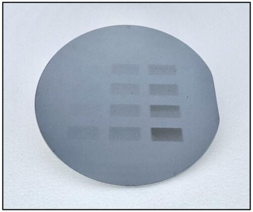
The research, published in Nature Chemical Engineering, demonstrates the first successful large-scale deposition of imidazole-based metal-organic resists from solution. The methodology can be precisely engineered and enables rapid exploration of different metal-organic combinations.
“By playing with the two components (metal and imidazole), you can change the efficiency of absorbing the light and the chemistry of the following reactions. And that opens us up to creating new metal-organic pairings.”
The Zinc Advantage
Different metals perform better at different radiation wavelengths, creating opportunities for wavelength-specific optimization. Zinc, which performs poorly with current extreme ultraviolet radiation, excels with B-EUV wavelengths. This wavelength specificity allows engineers to match materials to manufacturing requirements with unprecedented precision.
The research team has identified at least 10 different metals that could work with hundreds of organic compounds, creating a vast playground for materials development. They’ve already demonstrated successful films using cobalt-imidazole and zinc-benzimidazole combinations, proving the versatility of their approach.
Computational fluid dynamics models accurately predict the deposition process, enabling predictive design rather than trial-and-error development. The team achieved deposition rates of approximately 1 nanometer per second with excellent uniformity across centimeter-scale substrates.
The technique produces amorphous films with densities 70% higher than traditional crystalline materials, potentially offering superior performance characteristics. Films remained stable for months under ambient conditions, suggesting robust manufacturability.
Initial lithography tests using both electron beam and B-EUV radiation demonstrated successful pattern formation at feature sizes approaching current industry standards. The materials showed both positive and negative tone behavior depending on composition, providing flexibility for different manufacturing requirements.
While commercial implementation remains years away, the research establishes key groundwork for next-generation semiconductor manufacturing. The ability to precisely control material properties while maintaining compatibility with existing production equipment could accelerate adoption timelines.
Co-authors include researchers from East China University of Science and Technology, École Polytechnique Fédérale de Lausanne, Soochow University, Brookhaven National Laboratory, and Lawrence Berkeley National Laboratory, reflecting the international scope of advanced semiconductor research.
Nature Chemical Engineering: 10.1038/s44286-025-00146-3
ScienceBlog.com has no paywalls, no sponsored content, and no agenda beyond getting the science right. Every story here is written to inform, not to impress an advertiser or push a point of view.
Good science journalism takes time — reading the papers, checking the claims, finding researchers who can put findings in context. We do that work because we think it matters.
If you find this site useful, consider supporting it with a donation. Even a few dollars a month helps keep the coverage independent and free for everyone.