Scientists have discovered how to turn individual silicon molecules into electrical switches by harnessing quantum interference—the same wave-like behavior that makes noise-canceling headphones work.
The finding could enable a new generation of ultra-miniaturized electronics that embrace, rather than fight, the strange quantum effects plaguing today’s shrinking computer chips.
Researchers at the University of California, Riverside built silicon structures atom by atom from the bottom up, achieving precise control over electron flow through crystalline silicon at the molecular level. Their approach represents a fundamental shift from traditional chip manufacturing, which carves circuits into silicon wafers and has reached physical limits as components approach single-nanometer scales.
Molecular Noise-Canceling for Electrons
“We found that when tiny silicon structures are shaped with high symmetry, they can cancel out electron flow like noise-canceling headphones,” said Tim Su, a UCR chemistry professor who led the study. “What’s exciting is that we can control it.”
The key lies in a phenomenon called destructive quantum interference, where electrons behaving as waves can cancel each other out. By building silicon molecules with specific three-dimensional symmetries, the researchers created molecular switches that turn conductivity “on” or “off” depending on how electrodes align with the molecule’s internal pathways.
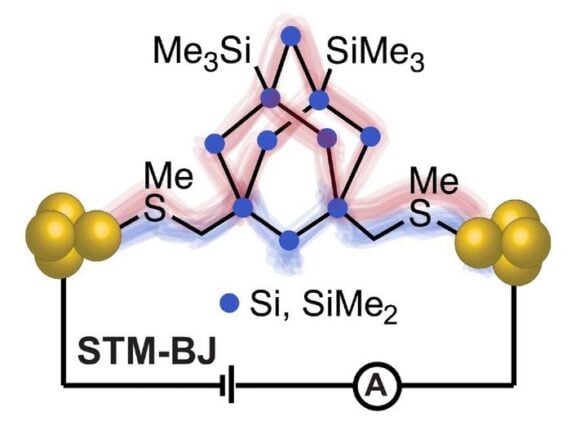
The study, published in the Journal of the American Chemical Society, focused on sila-adamantane—a diamond-shaped silicon molecule whose core structure mirrors the basic building block of crystalline silicon used in computer chips. Unlike previous research on simpler silicon chains, this three-dimensional architecture enabled unprecedented control over quantum transport.
Breaking the Silicon Scaling Wall
The discovery comes as the semiconductor industry confronts fundamental limits in traditional chip design. As transistors shrink below 10 nanometers, quantum effects like electron tunneling through insulating barriers make conventional silicon behavior increasingly unpredictable. Rather than viewing these quantum phenomena as obstacles, Su’s team demonstrates how they can become tools.
Key advantages of the quantum approach include:
- Atomic-level precision in controlling electron flow
- Switching ratios 5.6 times higher than previous molecular switches
- Reversible control using mechanical force at sub-angstrom scales
- Compatibility with familiar silicon-based manufacturing
The molecular switches work by exploiting the diamond structure’s C3 rotational symmetry, which allows electrodes to couple equally with three different internal pathways. When aligned with longer molecular bridges, quantum interference effects suppress electron transmission. When aligned with shorter pathways, conductivity increases dramatically.
Dynamic Quantum Control
Perhaps most remarkably, the researchers achieved reversible switching by applying mechanical force to stretch and compress individual molecular junctions. This represents the first demonstration of dynamically controlled quantum interference in silicon, with switching events occurring as molecular conformations change under mechanical stress.
The team used scanning tunneling microscopy to measure conductance through single-molecule junctions, applying sub-angstrom mechanical control to trigger conformational changes. Junction “training” through repeated stretch-compression cycles improved switching performance, suggesting these molecular devices could be optimized through use.
Electronic transport calculations revealed that the switching mechanism depends on how frontier molecular orbitals interfere with each other near the Fermi energy. In compressed configurations, destructive interference between molecular orbitals creates the “off” state. Stretching relieves this interference, restoring conductivity.
Beyond Traditional Electronics
The implications extend beyond conventional computing. The precise quantum control demonstrated here could advance thermoelectric devices that convert waste heat to electricity, or contribute to quantum computing components built from familiar materials rather than exotic alternatives.
“Our work shows how molecular symmetry in silicon leads to interference effects that control how electrons move through it,” Su explained. “And we can switch that interference on or off by controlling how electrodes align with our molecule.”
The research suggests that other conjugated silicon clusters with non-equivalent pathways could serve as quantum switching nodes, where resistivity changes by toggling which molecular bridges carry current. This “bottom-up” molecular approach could complement traditional “top-down” chip manufacturing as both converge at the nanoscale frontier.
While practical applications remain years away, the work establishes fundamental principles for quantum-controlled electronics using silicon—the semiconductor industry’s most familiar material. As quantum effects become unavoidable in ultra-small devices, learning to harness rather than suppress them may determine the future of computing.
ScienceBlog.com has no paywalls, no sponsored content, and no agenda beyond getting the science right. Every story here is written to inform, not to impress an advertiser or push a point of view.
Good science journalism takes time — reading the papers, checking the claims, finding researchers who can put findings in context. We do that work because we think it matters.
If you find this site useful, consider supporting it with a donation. Even a few dollars a month helps keep the coverage independent and free for everyone.