At around 470 degrees Celsius, something shifts inside the thin film. The atoms of bismuth, iron, and oxygen that had arranged themselves in a rhombohedral lattice, a slightly squashed cube that tilts at an angle, begin to slip into a new configuration. The structure tips sideways into what crystallographers call monoclinic. It is a subtle rearrangement, barely visible even with X-ray diffraction equipment, but the electrical consequences are anything but subtle. The film’s ability to convert a squeeze into a voltage, or a voltage into movement, jumps by more than a factor of five.
That structural trick, exploited by Takeshi Yoshimura and his colleagues at Osaka Metropolitan University, may help solve one of the longer-running irritants in consumer electronics. The most efficient piezoelectric materials, which are common in everything from microphones to sonar, rely on lead compounds. Lead zirconate titanate, known almost universally as PZT, has dominated the field for decades. It works beautifully, but it is toxic, accumulates in the environment, and is increasingly subject to regulatory pressure across Europe and Asia. The industry has been searching for a viable replacement that does not require redesigning the entire manufacturing infrastructure it already depends on.
Bismuth ferrite has long looked promising on paper. It is entirely lead-free, and early measurements suggested it could rival PZT’s piezoelectric performance. The practical problem is that bismuth ferrite films grown on silicon wafers, the kind you find in virtually every semiconductor fab on earth, have consistently underperformed. The reason is mechanical. When a bismuth ferrite film cools after deposition, silicon pulls on it in a way that stretches the crystal structure. Compressive strain, the kind that researchers can induce by growing films on specially chosen oxide substrates in the laboratory, tends to push bismuth ferrite’s atomic geometry toward configurations that are highly piezoelectrically active. Silicon pulls it the wrong way.
Yoshimura’s group decided to stop fighting that pull. “Rather than trying to avoid tensile strain,” he says, “we tried to use it to our advantage.” The question was whether tensile strain, correctly controlled, could force a different but equally useful phase transition: not rhombohedral to tetragonal as compressive strain typically does, but rhombohedral to monoclinic. Theory suggested it might. Getting there required precise control of temperature and film chemistry during deposition, two variables that interact in complicated ways.
The team introduced a small amount of manganese into the bismuth ferrite, a move that turned out to do something previously unappreciated. Undoped bismuth ferrite on silicon snaps almost immediately into the monoclinic configuration as it cools, leaving no room to study how the transition affects electrical properties. Manganese doping stabilised the original rhombohedral structure enough that both phases could coexist across different parts of a single wafer, depending on exactly where the temperature gradient happened to put each region. That accident of stabilisation gave the researchers a map. By studying how properties changed across the wafer, they could identify precisely where the rhombohedral-to-monoclinic boundary produced the best electrical output.
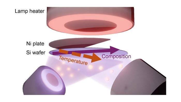
Finding that sweet spot efficiently required a method the group calls biaxial combinatorial sputtering. “This approach enabled dozens of growth conditions to be tested simultaneously,” Yoshimura says, “dramatically accelerating optimization compared with conventional trial-and-error methods.” Conventional thin-film deposition would require growing, cooling, characterising, and discarding dozens of individual wafers to explore the same parameter space. Here, one wafer could carry a systematic library of compositions and temperatures at once, effectively running parallel experiments on a single substrate. The technique is adapted from approaches used in pharmaceutical and catalyst discovery, but it is relatively unusual in piezoelectric device research.
The optimised films achieved a piezoelectric coefficient of -6.0 C per square metre, the highest yet recorded for any bismuth ferrite based material. That figure matters because it directly determines how much electrical charge a film produces per unit of mechanical stress applied to it. PZT films typically exceed -20 C per square metre on this metric, so bismuth ferrite is still not a like-for-like replacement in every application. But for energy harvesting, where a different figure of merit matters, the Osaka material actually pulls ahead. The relevant metric combines the electromechanical coupling factor with the mechanical quality factor, which together determine how efficiently a device extracts power from environmental vibrations. The BFMO devices reached a figure of merit of 2.7, compared to 1.9 for PZT-based harvesters in the same test.
The practical demonstration was a cantilever device, a 7-millimetre arm that flexes when shaken and generates a voltage as it does. Under steady sinusoidal vibration it delivered power approaching ninety-eight percent of the theoretical maximum. Under impulsive forces, the kind produced by machinery start-stops, door slams, or footsteps, the devices also performed well, though for a slightly different reason. The BFMO cantilever dampened its vibrations to ten percent of peak output in roughly 1.2 seconds after each impact. A comparable undoped bismuth ferrite device took 3.4 seconds to do the same. That quick decay matters: the device is ready to harvest again three times faster, which translates directly into higher average power output in environments where impacts are intermittent rather than continuous.
There is a practical argument for the BFMO approach that goes beyond performance numbers. The entire fabrication process uses sputtering on standard silicon wafers, a technique already running in semiconductor factories worldwide. “Although piezoelectric materials are already everywhere around us,” Yoshimura says, “the highest-performing ones still rely on lead, which is bad for the environment.” Getting a lead-free material that performs competitively and slots into existing manufacturing lines without demanding new equipment or processes is, from an industrial standpoint, arguably more useful than a laboratory curiosity that requires exotic substrates.
Whether the material eventually finds its way into wireless sensors, implantable medical devices, or the countless IoT nodes that engineers are trying to power without cables or batteries will depend on how well the performance holds across production batches and over long operating lifetimes, questions the Osaka group has not yet addressed at scale. The electromechanical coupling also drops slightly during MEMS device fabrication, from -6.0 to -5.1 C per square metre, suggesting that the etching and patterning steps needed to build real devices take a small toll on the crystal structure.
Still, the underlying physics is now clearer than it was. Tensile strain on silicon, long treated as an obstacle to good piezoelectric performance, turns out to be a lever. The monoclinic phase boundary that manganese doping makes accessible is where the interesting electrical activity happens. The next challenge is learning how to park the material at that boundary reliably, at scale, and keep it there.
DOI / Source: https://doi.org/10.1038/s41378-026-01177-5
—
Frequently Asked Questions
Lead zirconate titanate has dominated high-performance piezoelectrics for decades because it works exceptionally well, but lead compounds are toxic, persist in the environment, and face tightening regulations across Europe and Asia. As piezoelectric devices become more common in sensors, IoT hardware, and energy harvesters, the volume of lead involved grows, and so does the pressure on manufacturers to find alternatives that perform comparably without the environmental liability.
Piezoelectric materials generate an electric charge when their crystal lattice is mechanically deformed. Press on the material and its internal structure distorts, displacing positive and negative ions relative to each other and creating a voltage. In a vibration energy harvester, a cantilever flexes with each vibration cycle, continuously squeezing and releasing the piezoelectric film and generating alternating current that can be rectified and stored. The efficiency of that conversion depends on how strongly the material’s atomic geometry couples mechanical strain to electrical output.
The piezoelectric effect is fundamentally about geometry. Certain crystal arrangements create much larger internal voltage shifts for a given amount of strain than others. Bismuth ferrite near the boundary between its rhombohedral and monoclinic phases has more freedom to deform along multiple crystal directions simultaneously, which amplifies the electrical response. The Osaka group essentially learned to position their films at that boundary, rather than on either side of it, which is where the highest performance lives.
That is the target application, though it is early. The films produced power approaching the theoretical maximum under lab vibration conditions, and the quick damping after impacts means the device resets rapidly for the next energy harvesting cycle. The fabrication is already compatible with standard semiconductor manufacturing. What remains unclear is long-term reliability over millions of flex cycles, performance consistency across large production batches, and how the material behaves in the temperature and humidity ranges that real-world sensors actually experience.
Most advanced piezoelectric research uses specialised oxide substrates, which produce excellent results in the laboratory but cannot be integrated into the semiconductor fabs that make consumer electronics. Demonstrating the same physics on ordinary silicon, using sputtering equipment that fabs already operate, removes one of the largest barriers between a promising material and a manufacturable product. A lead-free piezoelectric that requires entirely new equipment to produce would face a much steeper adoption curve than one that slides into existing production lines.
ScienceBlog.com has no paywalls, no sponsored content, and no agenda beyond getting the science right. Every story here is written to inform, not to impress an advertiser or push a point of view.
Good science journalism takes time — reading the papers, checking the claims, finding researchers who can put findings in context. We do that work because we think it matters.
If you find this site useful, consider supporting it with a donation. Even a few dollars a month helps keep the coverage independent and free for everyone.