Ruthenium dioxide is not a material that makes headlines. A grey, conductive oxide used mainly as an electrode coating in industrial electrolysis cells, it’s the kind of workhorse compound that materials scientists know well and the rest of us never think about. Yet in a basement laboratory at the University of Minnesota, a thin film of this unremarkable metal oxide has just done something that should not, strictly speaking, be possible: it developed an electric polarisation.
Polarisation, the separation of positive and negative charge across a material, is the defining property of ferroelectrics, the ceramics used in sensors, actuators and memory devices. In metals, it cannot exist. Or so the received wisdom went. Free electrons in a conductor screen out any internal electric field almost instantaneously, collapsing whatever charge separation might momentarily form. The idea of a polar metal was considered a near-contradiction, a bit like a transparent mirror. Metals conduct; ferroelectrics polarise. They don’t do both.
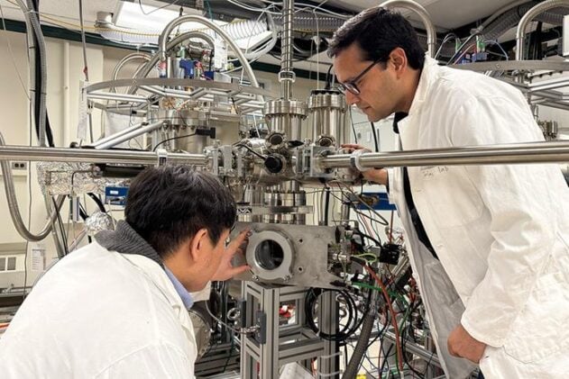
Bharat Jalan, a professor of chemical engineering at Minnesota, has been chipping away at that assumption for years. His group works with ultrathin oxide films grown atom-by-atom under carefully controlled conditions, and what they have found in RuO2 suggests the rule about metals and polarisation needs substantial revision. “We often think of polarization as something that belongs to insulators or ferroelectrics, not metals,” Jalan says. “Our work shows that, through careful interface design, you can stabilize polarization in a metallic system and use it as a knob to tune electronic properties. This opens an entirely new way of thinking about controlling metals.”
A Thickness That Changes Everything
The key, it turns out, is thickness. And the magic number is roughly 4 nanometres.
When a thin RuO2 film is grown on top of titanium dioxide (TiO2), the two crystal lattices don’t quite line up. The ruthenium oxide wants to adopt its natural spacing, but the titanium dioxide substrate holds it under strain, forcing the atoms into a slightly compressed arrangement. At film thicknesses below about 4 nm, that strain is strong enough to persist throughout the layer. Above that threshold, the film begins to relax, growing misfit dislocations and reverting towards its natural structure. Unremarkable in itself; this kind of strain relaxation is a routine feature of thin-film growth. What Jalan’s group discovered is what happens at the interface during that strained phase, and what it does to the material’s electronic behaviour.
Using a technique called multislice electron ptychography, an imaging method that reconstructs atomic positions from scattered electron beams with sub-angstrom precision, the team was able to map where atoms actually sat within the crystalline structure at the RuO2/TiO2 boundary. The images revealed something unexpected: at each interface, the ruthenium and titanium ions were displaced slightly from where they should be, nudged a few picometres (trillionths of a metre) off-centre relative to the surrounding oxygen atoms. Small displacements. But in a consistent direction, pointing from the TiO2 into the RuO2, and pointing the other way at the opposite interface. Electric dipoles, in a metal.
A Lever No One Knew Existed
The consequences for the surface work function were striking. Work function is the energy it takes to pull an electron out of a material’s surface, a parameter that governs how well a material injects charge into adjacent layers and how it interacts with catalytic reactions. For most metals, tuning the work function by a few tenths of an electron volt requires chemical treatments, adsorbing molecular layers onto the surface, exposing it to reactive gases or irradiating it with light. Jalan’s films, by simply adjusting thickness from below 4 nm to above it, showed a work function shift exceeding 1 electron volt. That figure places them in the same league as molecule-adsorption studies on gold and platinum surfaces, without any surface chemistry at all.
Seung Gyo Jeong, the paper’s first author, was the one doing most of the hands-on work, and he sounds like someone who has not quite finished being surprised by what they found. “We expected subtle interface effects, but not such a large and controllable change in work function,” he says. “Being able to visualize the polar displacements at the atomic scale and connect them directly to electronic measurements was especially exciting.”
The mechanism Jalan and Jeong propose goes something like this. The strained TiO2 layer adjacent to the RuO2 develops a polarisation under the mechanical stress of lattice mismatch, because its crystalline symmetry gets broken at the interface. That polarisation propagates a short distance into the conducting RuO2 layer, inducing a small internal electric field before the metal’s free electrons screen it out. The field shifts the effective energy landscape at the RuO2 surface, raising the work function. When the film relaxes past about 4 nm, the mechanical strain that was sustaining the polarised TiO2 dissipates, the internal field collapses, and the work function drops back. Thickness is the switch; strain is the mechanism.
From Lab Bench to Device Stack
The practical implications range across rather a lot of territory. Work function is arguably the single most important surface parameter in electronics: it determines the barrier height at transistor contacts, governs charge injection in organic light-emitting devices, and controls the energy threshold for catalytic electron transfer. The ability to tune it by more than 1 eV, without surface treatment, simply by choosing a film thickness, is the sort of design handle that engineers building next-generation logic circuits or electrocatalytic reactors would quite like to have. The effect also opens the door to approaches that bury a polarised layer inside a device stack, rather than engineering the surface itself, which could provide a more stable and scalable route to work function engineering. Buried interfaces don’t corrode, don’t desorb, and don’t depend on ambient chemistry.
There are limits. The effect is largest in the strained regime, below the 4 nm critical thickness, which also happens to be where the films are ultrathin and consequently more difficult to integrate into real device architectures. The work is also confined so far to one material system (RuO2 on TiO2), and whether the same physics will operate in other polar metal candidates is a question the group hasn’t yet answered. Given how recently the concept of a polar metal went from theoretical curio to experimentally verified phenomenon, though, that question seems less like an obstacle than an invitation. Jalan’s team has demonstrated that polarisation and conductivity can not only coexist in a metal, but be tuned against each other by design. What other combinations might be possible is, for now, anyone’s guess.
Read the full study in Nature Communications
Frequently Asked Questions
Why can’t metals normally have electric polarisation?
In a conventional metal, free electrons move so quickly that they screen out any internal electric field almost instantly, preventing the charge separation that polarisation requires. Polarisation is the signature property of insulators and ferroelectrics, not conductors, which is why the discovery of a stable polarised state in metallic ruthenium dioxide is so significant. The trick, it seems, is to use mechanical strain at an interface to force the effect into existence before the electrons can fully suppress it.
What is work function and why does tuning it matter for electronics?
Work function is the minimum energy needed to pull an electron free from a material’s surface, and it controls how easily charge flows between adjacent layers in a device. Getting the right work function match between a metal contact and a semiconductor is critical for transistors, solar cells and LEDs, yet tuning it usually requires applying chemical coatings or reactive gases. A method that adjusts work function by more than 1 electron volt just by changing film thickness could simplify the engineering of electronic and catalytic devices considerably.
Could this technique be used in real devices anytime soon?
The effect is strongest in films thinner than about 4 nanometres, which presents real integration challenges for conventional manufacturing. The researchers have demonstrated the principle in a single material pair so far, and extending it to other oxide systems will require further work. That said, buried-interface approaches are generally more stable than surface modifications, so if the physics proves transferable, it could eventually offer a durable route to work function engineering in transistors, electrodes and quantum devices.
How did researchers actually see atoms being displaced inside a conducting material?
The team used multislice electron ptychography, a computational imaging technique that reconstructs atomic positions from the way electrons scatter through a sample in a scanning transmission electron microscope. Because it can locate both heavy metal ions and lighter oxygen atoms with high precision, it was possible to measure displacements of just a few picometres at the interface, revealing the electric dipoles that no one had previously been able to directly observe in a metallic system.
ScienceBlog.com has no paywalls, no sponsored content, and no agenda beyond getting the science right. Every story here is written to inform, not to impress an advertiser or push a point of view.
Good science journalism takes time — reading the papers, checking the claims, finding researchers who can put findings in context. We do that work because we think it matters.
If you find this site useful, consider supporting it with a donation. Even a few dollars a month helps keep the coverage independent and free for everyone.