

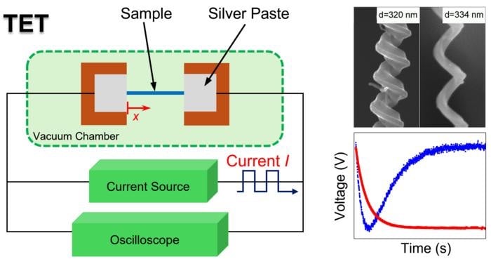
Take a platinum wire twenty-five micrometres across, which is roughly a quarter the width of a human hair, and suspend it in a vacuum between two aluminium electrodes. Apply a pulse of electrical current. For the next few seconds, the wire warms, its resistance climbs, and the voltage across it shifts in a way that encodes, precisely, how fast heat moves through the metal. That is essentially the whole experiment. The elegance of it is almost irritating.
What Xinwei Wang’s group at Iowa State University developed from this idea back in 2007 has, in the nearly two decades since, grown into something considerably more consequential than a clever lab trick for measuring platinum wires.
The technique is called transient electro-thermal measurement, or TET, and a comprehensive review published in the journal Thermo-X lays out just how far it has come. It can now measure the thermal properties of materials ranging from conventional millimetre-scale fibres down to sheets of graphene a single atom thick, and it does so with uncertainties below one percent under optimised conditions. That combination, broad applicability and genuinely high accuracy, is rarer than it sounds. The thermal characterisation field has no shortage of methods, each with its own workarounds, caveats, and approximate assumptions.
Why Measuring Heat in Thin Materials Is Harder Than It Looks
The problem is this: when you shrink a material down to nanoscale dimensions, the methods you would use on a bulk sample start to fail in ways that are difficult to correct for. Laser-based techniques such as time-domain thermoreflectance require the sample surface to be coated in metal and polished to a specific smoothness. Raman thermometry, which infers temperature from the frequency shift in scattered light, cannot be applied to metallic or centrosymmetric materials, and accurately measuring how much laser power is actually absorbed is, as anyone who has attempted it will tell you, genuinely tricky. The suspended micro-bridge approach, a classical method for one-dimensional materials like nanowires and fibres, requires microfabrication steps that are time-consuming and imposes serious difficulties in evaluating thermal contact resistance at the junctions. Each technique has its niche. None of them does everything cleanly.
TET sidesteps many of these complications by using the material itself as both heater and thermometer. Because the electrical resistance of most conducting materials changes predictably with temperature, the voltage-time trace produced during a pulse of current carries all the thermal information needed. There is no laser to align, no reflective coating to deposit, no complex optical calibration. The sample is suspended in vacuum to eliminate convection, and the electrodes act as heat sinks that define the boundary conditions. The physics, as a result, reduces to a clean one-dimensional heat diffusion problem that can be solved analytically, and the thermal diffusivity extracted from the resulting curve with, in principle, high fidelity.
The platinum wire validation tells you roughly how well it works in practice. Using a method that extrapolates measurements taken at several different heating currents back to zero temperature rise, which eliminates the complicating effect of the wire running hotter than the ambient temperature you are actually trying to characterise, the team achieved agreement with the accepted literature value to within about 0.6%. For a thermal measurement, that is a result that commands a degree of respect.
When the Sample Is Thinner Than the Method
The more interesting territory begins when the material under study becomes too thin to suspend independently. A few-layer graphene sheet, for instance, is not going to hold itself up between two electrodes; it needs support. The TET group’s solution is to mount the graphene on an ultra-thin polymer film, around 700 nanometres of poly(methyl methacrylate), and measure the composite. Then, by subtracting the polymer’s known thermal contribution, you can recover the graphene’s thermal conductivity. The approach requires careful accounting, but the differential method is well enough understood that thermal conductivities down to around 33 watts per metre kelvin have been measured on graphene samples, an accuracy that the review paper argues is considerably better than Raman-based methods typically manage.
Going thinner still, the technique has been pushed to iridium films with average thicknesses of 0.6 nanometres, which is perhaps five or six atomic layers depending on orientation. At that scale, the thermal and electrical conductivities of the iridium are reduced by roughly 80 and 50 percent respectively compared to bulk values, and the Lorenz number, a fundamental ratio linking thermal and electrical transport in metals, comes out at nearly twice the bulk value. These are not marginal corrections to known physics; they suggest that electrons near boundaries scatter in ways that bulk measurements cannot capture, and that the widely used Wiedemann-Franz law breaks down at the nanoscale in quantifiable ways.
The technique’s capacity to operate across extreme temperature ranges adds another dimension. Single-walled carbon nanotube films have been measured from room temperature all the way down to twelve kelvin, well below the temperature at which most metals behave in ways you might predict from textbooks. The thermal diffusivity of the film drops by a factor of around four between 290 kelvin and 12 kelvin, a trend that reflects the changing balance of phonon transport mechanisms as thermal energy falls. Getting accurate measurements at cryogenic temperatures turns out to require the same zero-temperature-rise extrapolation used for the platinum wire, for the simple reason that at low temperatures, you need a larger current pulse to generate a detectable voltage signal, and that pulse heats the sample away from the very temperature you wanted to measure.
Taking the Pulse of a Material as It Changes
Perhaps the least obvious application of TET is as a real-time monitoring tool. Because each measurement takes only a second or two, you can watch what happens to a material’s thermal properties as you process it. Graphene aerogel fibres, which have extremely low thermal conductivity to begin with, have been monitored continuously during laser photoreduction, a process that converts graphene oxide into something closer to pure graphene. The thermal diffusivity climbs steadily as the laser progressively removes oxygen groups and restores the carbon lattice. Biomass pyrolysis has been followed in the same way, tracking how thermophysical properties shift during the chemical decomposition of plant material. The temporal resolution is good enough to catch events that are over in minutes.
Carbon nanotube bundles provided what is perhaps the most conceptually striking finding. At room temperature, TET signals from these bundles are normal, a smooth voltage decay that fits a single thermal diffusivity. Cool the sample down to around 35 kelvin, and the signal splits into two distinct phases: a fast initial decay followed by a slower tail. The explanation involves the geometry of the bundles themselves. During chemical vapour deposition growth, some of the initially straight carbon nanotubes transform into coiled morphologies. At room temperature, heat moves easily between straight and coiled regions. At cryogenic temperatures, thermal contraction separates the two populations at the nanoscale, and they conduct heat at measurably different rates. The phenomenon would be almost impossible to detect with a steady-state measurement.
The field of two-dimensional materials, which now extends well beyond graphene to include transition metal dichalcogenides, hexagonal boron nitride, and a growing catalogue of other atomically thin sheets, increasingly needs thermal characterisation tools that can handle samples that are both nanoscale in thickness and difficult to suspend in free space. The differential TET approach appears to be well placed to meet that need, though the review’s authors note that the technique is, as yet, underutilised relative to Raman methods in the 2D materials community. Whether that changes will depend partly on whether the community grows comfortable enough with the experimental requirements, and partly on how clearly the accuracy advantage is communicated. The numbers, at least, make a fairly direct case.
https://doi.org/10.70401/tx.2025.0002
Frequently Asked Questions
What exactly does “thermal diffusivity” mean, and why does it matter?
Thermal diffusivity measures how quickly a material responds to a change in temperature, specifically how fast heat moves through it relative to its capacity to store heat. A high thermal diffusivity means heat spreads rapidly; a low value means the material responds slowly. This matters enormously for designing electronics, because a chip that cannot shed heat fast enough will overheat, and for energy storage and thermal management systems, where controlling heat flow is the central engineering challenge.
Why is it so hard to measure thermal properties in ultrathin materials?
At nanoscale thicknesses, the material represents only a tiny fraction of any composite system you measure, so the signal you are trying to detect is easily swamped by contributions from supporting layers or substrates. Many standard techniques also require surface coatings, precise laser alignment, or microfabricated structures that become impractical at sub-nanometre scales. The TET approach gets around this by using the material’s own electrical response to infer temperature, but even then, careful subtraction of supporting-layer contributions is essential.
Could this technique be used outside the laboratory, in industrial settings?
The experimental setup is relatively straightforward compared to laser-based alternatives, which makes it more plausible as an industrial tool. The review paper identifies additive manufacturing, polymer curing, and phase-change materials for thermal management as possible application areas, where real-time monitoring of thermal properties during processing could improve quality control. The main barrier is sample preparation: the material needs to be suspended or supported in a controlled way, which rules out many intact manufactured components.
What does the Lorenz number finding tell us about nanoscale materials?
The Lorenz number relates how well a material conducts heat to how well it conducts electricity. In bulk metals, this ratio is approximately constant, a result called the Wiedemann-Franz law. At the nanoscale, grain boundaries and surfaces scatter electrons differently depending on whether they are carrying heat or charge, so the ratio changes. Finding that a 0.6-nanometre iridium film has a Lorenz number nearly twice the bulk value tells us that standard bulk transport theory cannot simply be scaled down, and that new physics governs how electrons behave in atomically thin conductors.