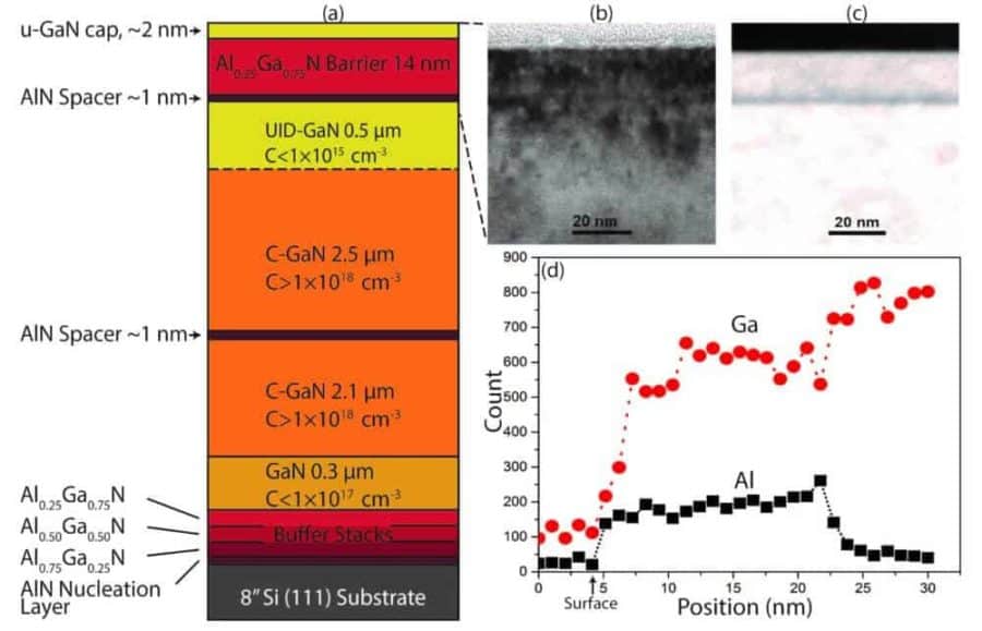
A team of researchers at the University of Illinois at Urbana-Champaign has advanced gallium nitride (GaN)-on-silicon transistor technology by optimizing the composition of the semiconductor layers that make up the device. Working with industry partners Veeco and IBM, the team created the high electron mobility transistor (HEMT) structure on a 200 mm silicon substrate with … Read more…
ScienceBlog.com has no paywalls, no sponsored content, and no agenda beyond getting the science right. Every story here is written to inform, not to impress an advertiser or push a point of view.
Good science journalism takes time — reading the papers, checking the claims, finding researchers who can put findings in context. We do that work because we think it matters.
If you find this site useful, consider supporting it with a donation. Even a few dollars a month helps keep the coverage independent and free for everyone.